
Wide Band Gap Semiconductors
A material is classified as an insulator, semiconductor, or conductor based on the band gap (energy level) that separates the outermost orbit of the conduction band from the valance band. The insulator has the largest band gap, semiconductor has a medium band gap and the conductor has a lowest band gap.
In the field of electrical engineering, the conductor is used for transferring power from one location to other location, the semiconductors are used for switching in power conversion and the insulators are used for insulating the conductor to provide protection against leakage and ensures safety. And the capability of power transfer depends on the power handling capacity of the power conversion equipment made from the semiconductor.
For decades, the silicon is used as the semiconductor in the power conversion system. It has the band gap of 1.1 ev. Due to the emergence of more and more appliances and shift towards the use of electricity, the silicon-based systems are reaching it maximum performance limit. The research on semiconductor have produced better withstanding capability, better switching frequency, higher thermal handling capability and higher power density wide band gap materials. The higher withstanding capability can lead to high power design. Higher power density makes improvement in performance with decreased form factor and weight. Also it can work at higher temperature, with low carbon emission. All these leading to higher efficiency and low cost. Therefore, the device based on wide band gap technologies offers higher benefits than device based on silicon. Figure 1 displays the characteristics of the wide band gap semiconductors.
Silicon carbide (SiC), silicon dioxide (SiC), gallium nitride (GaN), boron nitride (BN), zinc oxide (ZnO), and diamond are examples of materials with wide band gaps. However, SiC and GaN are the most widely utilized wide band gap semiconductors. The band gap is the primary characteristic that contributes to its broad band gap. Their respective band gaps are 3.2 and 3.4 eV, which are about three times greater than silicon’s. This indicates that, despite potential differences in material preparation procedures, it can function at higher voltages and frequencies with reduced conduction and switching losses. Reduced losses lead to less thermal stress, extending the material’s life and dependability.
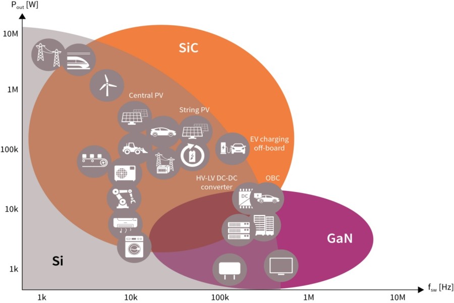
The GaN has 2,000 cm2/Vs of electron mobility, whereas SiC has 650 cm2/Vs of electron mobility. Therefore, electron mobility of GaN is 30% higher than SiC. This indicates that the capacitance is low and appropriate for high performance and high frequency operation due to the extremely minimal loss at the gate electrode. GaN can therefore be utilized in gigahertz-range radio frequency devices. However, the SiC is better suited for greater-power applications, such as the higher-end voltages needed in EVs and data centers, because of its higher thermal conductivity and lower frequency functioning. Additionally, the 650V-rated GaN is tailored for applications up to 20kW and provides faster switching, cheaper costs, and integration. SiC performs best at temperatures and voltages above 1,000V, making it ideal for devices and applications up to 20MW.
Advantages
- It can eliminate up to 90% of power losses, withstand voltages ten times greater, operate at least ten times higher frequency and twice high temperature than normal band gap material.
- The power electronic components made using wide bandgap semiconductor materials can be smaller, faster, more dependable, and more efficient.
Disadvantages
- It requires the development of cutting-edge manufacturing processes at affordable cost.
- It requires redesigning of device design to make it suitable for use in high thermal and high-power ratings applications.
Application
- Light in the visible color spectrum is emitted by the materials with wide band gaps and are used in solid-state lighting. For instance, light emitting diodes (LEDs) with extremely high efficiency are made possible by gallium nitride (GaN).
- Higher-efficiency variable frequency drives are based on wide band gap MOSFETs and IGBTs and are used in blowers, pumps and HVAC systems. They are also utilized in high-efficiency data centers, electric traction and small power supplies for consumer gadgets.
- Homes and businesses’ solar inverters use wide band gap-based power electronics switches, which cut losses by half. They are also employed in solid state transformers which reduced the size of it by a factor of 10 or more.
- Wide band gap-based power electronics switches are used in High-voltage DC power lines with reduced losses than high-voltage AC transmission lines.
Source: