
Powering up the future with GaN
The adoption of next-generation semiconductor material Gallium Nitride (GaN) in power-conversion devices, replacing conventional silicon chips, holds significant promise in achieving net-zero carbon emissions goals. Various industries, including automotive and telecommunications, are under increasing pressure to invest in more efficient power conversion and electrification due to stricter regulations and growing social demands for reduced CO2 emissions.
Conventional silicon-based power semiconductors like Insulated-Gate Bipolar Transistors (IGBTs) have limitations in terms of frequency, speed, and performance at high temperatures and low current levels. High-voltage Silicon Field-Effect Transistors (FETs) also face constraints in terms of frequency and high-temperature operation. To overcome these limitations, designers are increasingly turning to wide-bandgap (WBG) semiconductors with effective copper-clip packaging.
Efforts to enhance efficiency include increasing the effective threshold voltage (VT) to 3 V to align with readily available gate drivers. Integration features, such as a Miller clamp for high dV/dt operation and an integrated Kelvin and source current sensor for gate monitoring, eliminate the need for an additional source resistor. This allows for a direct connection of the low-side FET source pad to the ground plane, improving cooling.
The global push for net-zero carbon emissions by 2050 necessitates increased productivity in electric mobility, renewable energy generation, and data-intensive technologies like cloud computing and 5G. More efficient energy production is critical to meet these climate goals, leading to substantial investments of over $10 billion in WBG technology by the semiconductor industry.
The amount of energy used by humans is increasing. The world consumed 23,000 TWh of energy in 2019, which resulted in an increase of 36.7 Gt of CO2 in the atmosphere. The goal of net-zero CO2 emissions by 2050 can only be reached by investing in cleaner energy production and conversion. In order to achieve this, productivity must rise in the critical areas of electric mobility, the creation of renewable energy, and data-intensive software programs like cloud computing and 5G. More efficient energy production is required to meet climate change goals. As a result of this initiative, the semiconductor industry has invested over $10 billion in WBG technology.
GaN power devices perform better than traditional silicon devices when compared to the key figures of merit (FOM) for a specific voltage rating. For example, if the specific on-state resistance RDS(on) area (m-cm2) is less than half, the power density can be increased. Due to switching metrics like RDS(on) QG, the gate charge, is an order of magnitude more efficient at higher frequencies, especially at light loads, and enables faster switching.
The majority of the reverse-recovery charge is deposited on the QOSS output capacitance of GaN FETs. GaN’s lower RDS(on) QOSS allows for better soft-switching and lower switching losses. It is possible to use the GaN high electron mobility transistor (HEMT) in bridgeless totem pole topologies for power factor correction (PFC) stages that are more efficient and less expensive because it is unipolar and has a reverse recovery charge QRR of zero.
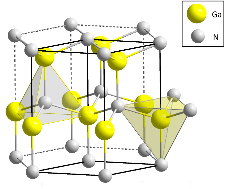
GaN devices
In terms of GaN devices, the inherent depletion-mode nature of GaN HEMTs has led to innovative solutions to make them normally-off devices, ensuring they are off when not actively driven. Two approaches include the use of a cascade arrangement, integrating a silicon low-voltage device with GaN, and employing a p-GaN gate to create an enhancement-mode (e-mode) device. While the cascade structure offers good gate control with higher threshold voltages from the silicon device, p-GaN gate HEMTs have a lower turn-on threshold and can operate with lower maximum gate voltages. Combining the advantages of both approaches, the ICeGAN structure by CGD integrates GaN circuitry to increase the threshold VT to 3.0 V, offering simplicity, lower system costs, and gate robustness. It is compatible with most commercial gate drivers, and its gate voltage is limited to 6 V by an internal gate clamp circuit, enhancing gate reliability, especially in response to temperature changes. Due to more stringent rules and increased social pressure to reduce CO2 emissions, a number of businesses, notably the automotive and telecommunications sectors, are under increasing pressure to invest in more efficient power conversion and electrification.
Additional features of ICeGaN include integrated Kelvin source sensing for improved heatsinking and a Miller clamp for smooth gate turn at high dV/dt transitions. It is recommended to position the gate driver outside the GaN package to prevent thermal interference with the power device. The device also supports dV/dt control, also known as slew rate control.
Source
- https://epc-co.com/epc/gallium-nitride/what-is-gan
- https://gansystems.com/gallium-nitride-semiconductor/
- https://www.powerelectronicsnews.com/enabling-the-future-of-power-electronics-yes-we-gan/